
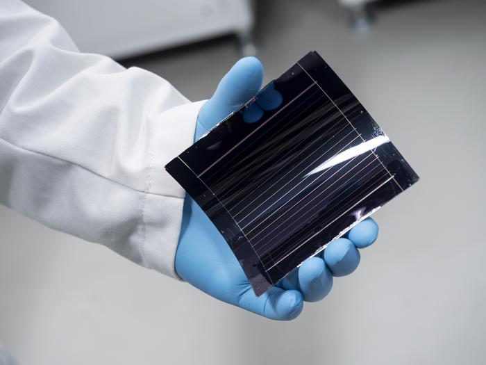
Despite its promise of good conversion efficiencies and relatively low costs, copper indium gallium diselenide (CIGS) photovoltaic technology has never been able to compete with crystalline silicon and has largely remained confined to the niche building-integrated photovoltaics (BIPV) market.
High-efficiency laboratory processes for CIGS have so far failed to scale economically to high-throughput industrial manufacturing. For example, record CIGS cells are achieved under tightly optimized growth conditions with narrow compositional and thermal windows. Such precision is manageable on small laboratory substrates but becomes increasingly difficult on large areas where maintaining uniform stoichiometry, phase purity, and defect control requires complex vacuum infrastructure and careful inline monitoring. Small deviations lead to secondary phases and recombination-active defects, directly affecting yield.
“At industrial scale, economics are governed not only by efficiency but by throughput, yield, and capital intensity,” CIGS specialist Mirjana Dimitrievska told pv magazine. “Multistage co-evaporation or complex sputter–selenization routes are slower and more equipment-intensive than mainstream silicon processing. When combined with strong price pressure from crystalline silicon, these factors limit the economic translation of laboratory performance into high-volume production.”
According to Dimitrievska, the main constraints are manufacturing complexity and scale. CIGS requires multicomponent control of Cu, In, Ga, and Se, often under high-vacuum conditions, which increases capital expenditure and process sensitivity. Yield losses from shunts, non-uniformity, and interface defects raise effective cost per watt.
“In parallel, crystalline silicon has achieved massive economies of scale and dramatic cost reductions over the past decade,” she went on to say. “This continuously shifting benchmark has narrowed the window in which CIGS could establish a cost advantage. Without very high module efficiencies and stable high-throughput manufacturing, matching silicon’s cost structure remains challenging.”
Another big challenge in CIGS development is the difficulty of replacing cadmium sulfide (CdS) buffer layers with cadmium-free alternatives, which affects environmental compliance and commercial viability.
“CdS plays a multifunctional role in CIGS devices,” said Dimitrievska. “Beyond forming the junction, it passivates the absorber surface and provides favorable band alignment that supports high open-circuit voltage and fill factor. Replacing CdS with cadmium-free alternatives such as zinc oxysulfide, (Zn(O,S)), zinc magnesium oxide (ZnMgO), or indium sulfide (In2S3) is technically feasible, but these layers often introduce tighter band alignment tolerances and greater sensitivity to processing conditions.”
“While removing cadmium improves the environmental profile and regulatory perception, any instability or efficiency loss at the interface directly impacts bankability,” she added. “The absence of a universally robust drop-in replacement has therefore slowed full industrial transition despite clear environmental motivation.”
Another considerable technical issue is that defect density increase significantly when transitioning from small lab cells to full-size modules. “Scaling to module dimensions increases the probability of local compositional fluctuations, thickness variations, and temperature gradients during growth. Larger areas also require monolithic interconnection through scribing, which introduces additional edges, interfaces, and potential shunt paths. These factors statistically increase defect density and non-uniformity,” said Dimitrievska.
“Higher defect density enhances non-radiative recombination and can create leakage pathways, reducing open-circuit voltage and fill factor. Additional resistive losses from transparent conductive oxides and interconnects further widen the cell-to-module efficiency gap,” she also stated.
CIGS sensitivity to moisture ingress and alkali migration also complicates long-term module reliability compared to crystalline silicon. In fact, if CIGS absorbers benefit from controlled alkali incorporation, typically sodium, to achieve high efficiency, mobile species and metastable defect states can evolve under bias, illumination, or humidity, affecting junction properties. Moisture ingress, particularly at edges or poorly sealed regions, can accelerate interface degradation.
“Crystalline silicon modules are largely limited by packaging-related degradation mechanisms, whereas CIGS reliability also depends on maintaining stable absorber and interface chemistry,” said the CIGS expert. “When encapsulation and process control are optimized, long-term stability is achievable, but the margin for processing variation is narrower.”
According to Dimitrievska, CIGS is particularly well suited for applications where lightweight, flexibility, or aesthetic integration provides added value. These include building-integrated photovoltaics, curved or facade elements, lightweight rooftop installations with load constraints, transportation-related surfaces, portable power systems, and certain aerospace or high-altitude applications.
“In such markets, performance per weight or per available surface area can outweigh absolute cost per watt. Rather than competing directly with commodity silicon in large utility-scale installations, CIGS startups can target differentiated segments where its form factor and tunable properties offer system-level advantages,” she said.
As of the latest reported data, the world record for a CIGS module is in the 20% range, which places this technology close to competitive thin-film technologies and approaching the lower end of mainstream crystalline silicon modules.
“However, absolute efficiency is only one piece of the commercial equation,” said the researcher. “For broad commodity market competition, approaching the high-teens to 20% on full-area modules with consistent high yield is beneficial because it improves power output per area and helps reduce balance-of-system costs. Durability, long-term stability, encapsulation quality, resistance to environmental stress, and predictable field performance are equally critical. A module that is marginally higher in efficiency but suffers significant early‐life degradation, moisture sensitivity, or unpredictable outdoor behavior will not be commercially competitive.”
In specialized markets, such as lightweight or flexible applications, building-integrated PV, curved surfaces, or portable power, slightly lower efficiencies can be acceptable if the product delivers unique values such as lower W/kg, conformability, aesthetic integration, and demonstrates reliable long-term performance. In these cases, system value metrics like energy delivered over lifetime per installed cost and reliability in challenging environments can outweigh peak efficiency numbers.
Another critical factor affecting the CIGS technology is that it more susceptible to rare earth material supply chain issues. “CIGS does not rely on rare earth elements,” said Dimitrievska. “However, it depends on indium and gallium, which are byproduct metals primarily obtained from zinc and bauxite processing. Their supply is therefore linked to broader mining activities and can be sensitive to geopolitical and market fluctuations.”
“For very large deployment scales, availability and price volatility of these critical elements could become limiting factors,” she went on to say. “For niche or moderate-scale markets, current supply chains are generally manageable, but long-term terawatt-scale expansion would require careful resource planning and recycling strategies.”
Dimitrevska and a group of her colleagues at the Swiss Federal Laboratories for Materials Science and Technology (Empa) have recently investigated how CIGS could be optimally combined with perovskite solar technologies in tandem cells and modules.
The scientits argue that the research community should move beyond chasing incremental efficiency gains and instead prioritize the resilience, stability, and sustainability of photovoltaic materials. They also emphasize the need for long-term field studies to assess real-world performance.
“Silicon is not the best semiconductor for solar cells,” Dimitrievska pointed out. “However, this technology has been in development for over 70 years and has already been greatly optimized thanks to continuous research and investment. If research and industry work together, the same can be achieved for perovskite and CIGS.”
The research findings were presented in “Lessons from copper indium gallium sulfo-selenide solar cells for progressing perovskite photovoltaics,” published in nature energy.
This content is protected by copyright and may not be reused. If you want to cooperate with us and would like to reuse some of our content, please contact: editors@pv-magazine.com.
Popular content
Source link