
An international research team has proposed a perovskite solar cell architecture incorporating a thin tetraphenyl-porphine zinc interfacial layer to enhance surface potential, passivate defect states, and improve charge transport. The strategy leads to improved device efficiency and operational stability, enabling power conversion efficiencies exceeding 13%.
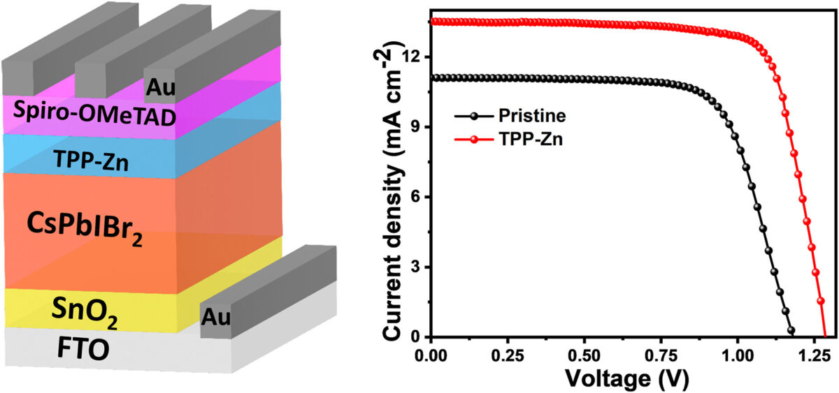
An international group of researchers has proposed a novel device design that enhances the surface potential of cesium lead iodide bromide (CsPbIBr₂) perovskite solar cells by depositing a thin layer of tetraphenyl-porphine zinc (TPP-Zn) onto the active layer.
Regular CsPbIBr₂ devices are well regarded for their superior operational stability compared to many other inorganic perovskite compositions, owing to their robust crystal lattice, reduced sensitivity to moisture, and improved thermal resilience. However, their practical application is still constrained by relatively low power conversion efficiencies, primarily linked to interfacial charge recombination and limited charge extraction.
“The novelty of this work lies in introducing a TPP-Zn interfacial layer to effectively modulate the surface potential and passivate trap states in all-inorganic wide-bandgap CsPbIBr2 perovskite solar cells,” corresponding author M. Bilal Faheem told pv magazine.
“Unlike conventional passivation strategies, the coordination interaction between TPP-Zn and undercoordinated metal cations enables simultaneous suppression of surface defects and enhancement of charge carrier dynamics, leading to improved device efficiency and stability,” he also explained. “Furthermore, the experimental outcomes were validated through an analogous simulation device design using SCAPS-1D against the photovoltaic parameters and thermal stability of perovskite solar cell devices.”
In fabricating the device, the researchers first cleaned fluorine-doped tin oxide (FTO) glass substrates and deposited a diluted tin(IV) oxide (SnO₂) electron-transport layer (ETL) via spin coating, followed by annealing at 100 C for 20 minutes and 150 C for 40 minutes. The CsPbIBr₂ perovskite absorber was then prepared by dissolving equimolar amounts (1.2 M) of cesium iodide (CsI) and lead bromide (PbBr₂) in dimethyl sulfoxide (DMSO). The solution was spin-coated onto the SnO₂ layer at 1,500 rpm for 20 seconds and 3,500 rpm for 60 seconds, followed by annealing at 200 C for 10 minutes.

Image: King Fahd University of Petroleum and Minerals (KFUPM), Materials Reports: Energy, CC BY 4.0
In the surface passivation step, a TPP-Zn solution in toluene was spin-coated onto the wet perovskite film at 5,500 rpm for 30 seconds, followed by annealing at 180 °C for 10 minutes. Subsequently, a hole-transport layer (HTL) of Spiro-OMeTAD was spin-coated on top. Finally, a 100-nm-thick gold (Au) electrode was deposited via thermal evaporation, yielding devices with active areas of 0.16 cm² and 1.02 cm². The final device architecture was FTO/SnO₂/CsPbIBr₂/TPP-Zn/Spiro-OMeTAD/Au.
The researchers used several methods to characterize the devices. X-ray diffraction (XRD) and ultraviolet-visible (UV-Vis) spectroscopy were used to study crystal structure, crystallinity, light absorption, and bandgap. At the same time, photoluminescence (PL) and time-resolved photoluminescence (TRPL) were used to analyze charge recombination and carrier lifetime.
Scanning electron microscopy (SEM), atomic force microscopy (AFM), Kelvin probe force microscopy (KPFM), and X-ray photoelectron spectroscopy (XPS) were then used to examine morphology, surface potential, and defect passivation. Device performance was tested using current density-voltage (J-V), incident photon-to-current efficiency (IPCE), Mott-Schottky, space-charge-limited current (SCLC), electrochemical impedance spectroscopy (EIS), and contact angle measurements.
The optimized CsPbIBr₂ PSC device was found to deliver a peak power conversion efficiency of over 13.47%, along with an open-circuit voltage of 1.29 V, a fill factor of 82.3%, and a short-circuit current density of 12.69 mA cm² for a device area of 0.16 cm². For the larger active area of 1.02 cm², the device maintains an efficiency of 11.29%. This simple yet effective approach provides a promising route toward the development of stable and high-performance inorganic perovskite solar cells.
“The most surprising result was the significant improvement in both efficiency and charge transport achieved with a simple, ultrathin TPP-Zn layer,” said Faheem. “Notably, the device demostrated that effective molecular-level passivation can substantially mitigate recombination losses in wide-bandgap inorganic perovskite-based PV devices.”
The device was described in “Surface engineered wide-bandgap all-inorganic perovskite solar cells achieve a fill factor exceeding 82%,” published in Materials Reports: Energy. Scientists from Saudi Arabia’s King Fahd University of Petroleum and Minerals (KFUPM), New York’s Syracuse University, Turkey’s Ankara Yıldırım Beyazıt University, China’s City University of Hong Kong, and Pakistan’s University of Narowal have participated in the study.
This content is protected by copyright and may not be reused. If you want to cooperate with us and would like to reuse some of our content, please contact: editors@pv-magazine.com.
Popular content
Source link